Introduction: Why This Matters
Everyone starts FPGA learning with a blinking LED. It works, it’s satisfying for about 30 seconds, and then you wonder — “what now?”
This post documents the next step: driving a real peripheral from an FPGA using nothing but pure hardware description language. No libraries. No Arduino. No microcontroller sitting in between. Just logic gates, a state machine, and a 16x2 LCD that had no idea what was coming.
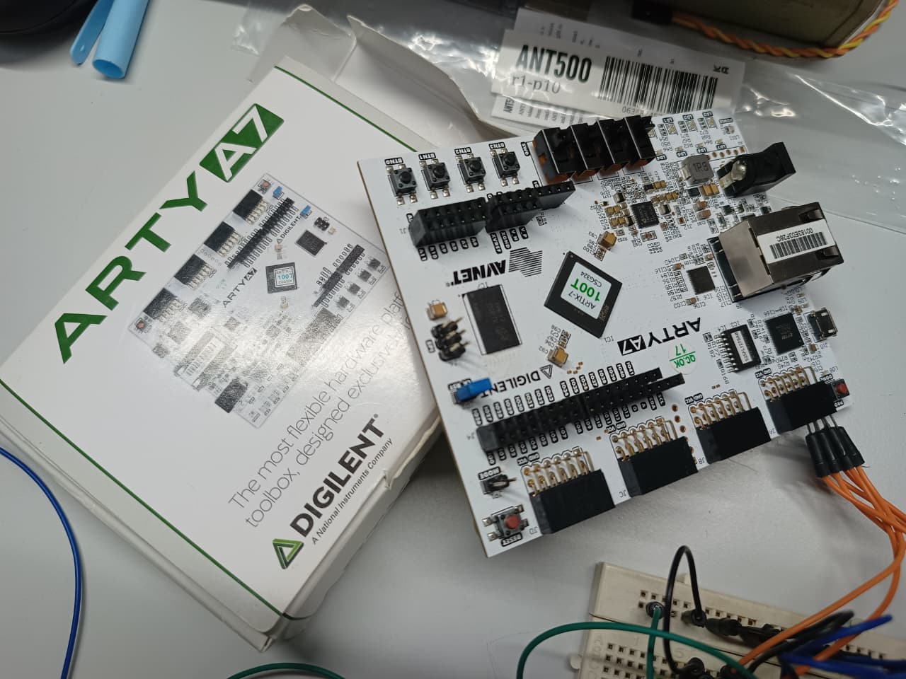
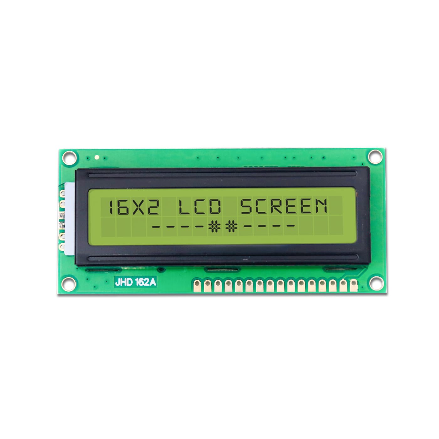
The board used is a Digilent Arty A7-100T (Xilinx Artix-7 FPGA, 100T variant). The display is a standard HD44780-based 16x2 green LCD. The tools are Vivado 2025.2 and SystemVerilog.
If you have ever wondered how a microcontroller’s lcd.print("Hello") actually works at the hardware level — this is exactly that, built from scratch.
Part 1: Background — What I Already Knew
Before this project, my FPGA experience was:
- One blink program on the Arty A7 (LED toggle, clock divider)
- An 8-bit ALU project from 2 years ago on a Numato Spartan-6 board using Xilinx ISE — simulation worked but the LED display never did
That old failure was actually a constraints file problem, not an HDL problem. XDC format on Vivado is completely different from UCF on ISE. Pin names change, I/O standards must be explicitly declared, and Vivado will refuse to generate a bitstream if even one port is unconstrained. That lesson paid off immediately here.
Coming from embedded systems (ESP32, STM32), the mindset shift for FPGA is significant:
- On an MCU, you write
delay(1000)— time is implicit - On an FPGA, there is no delay — you count clock edges explicitly
- Everything happens in parallel unless you design it to be sequential
- You are not writing a program — you are describing hardware
Part 2: Understanding the HD44780 — Why This Is Not Trivial
The HD44780 is the controller chip inside almost every cheap 16x2 LCD. It has been around since the 1980s and is incredibly common. But driving it from an FPGA is not the same as driving it from an Arduino.
On Arduino, the LiquidCrystal library handles everything invisibly. On an FPGA, you implement every step yourself.
The initialization sequence alone has 9 steps with specific timing:
- Wait >40ms after power-on before sending anything
- Send
0x3in 8-bit mode — wait 4.1ms - Send
0x3again — wait 150µs - Send
0x3again — wait 150µs - Send
0x2— switch to 4-bit mode - Function Set (
0x28): 2 lines, 5×8 font, 4-bit interface - Display On (
0x0C): display on, cursor off, blink off - Clear Display (
0x01): wait 1.52ms (slowest command) - Entry Mode (
0x06): increment cursor, no display shift
Miss any step or get the timing wrong — nothing displays. The LCD shows garbage or stays blank.
Why 4-bit mode?
The HD44780 supports 8-bit and 4-bit parallel interfaces. 8-bit uses 11 pins (RS, RW, E, D0–D7). 4-bit uses only 7 pins (RS, RW, E, D4–D7) by sending each byte in two nibbles. Since the Arty’s Pmod connector has 8 signal pins and we want to keep wiring simple, 4-bit mode is the practical choice.
The Enable pulse:
Every command or data byte is sent by:
- Setting RS (Register Select): 0 for command, 1 for data
- Putting the nibble on D4–D7
- Pulsing Enable (E) high for >450ns, then low
- Waiting for the LCD to process (37µs for most commands, 1.52ms for Clear)
At 100MHz, 450ns = 45 clock cycles. 37µs = 3700 clock cycles. The FSM must count these precisely.
Part 3: The Hardware Setup
What You Need
- Digilent Arty A7 (any variant) or any fpga baord like Numato Spartan 6,7 etc
- HD44780 16x2 LCD (parallel interface, no I2C backpack)
- Breadboard and jumper wires
- 10K resistor (R1) and 1K resistor (R2) for contrast voltage divider (you can use Poetntiometer i didn’t had that…)
- 100Ω resistor for backlight current limiting
Power Rail Warning
The LCD runs on 5V. The Arty A7 I/O is 3.3V.
The HD44780’s logic high threshold (VIH) is ~2.2V minimum, so 3.3V from the FPGA is sufficient to drive it. But the LCD’s VDD (power pin) must be 5V — connecting it to the Pmod’s 3.3V rail will cause the display to show nothing or behave erratically.
The Arty board has a 5V pin on its outer power header. Use that for LCD VDD.
Contrast Voltage Divider
The LCD’s V0 pin controls contrast. With a potentiometer you can tune it — without one, a resistor divider works fine.
Target voltage: 0.4V to 0.9V on V0.
Using 10K (R1) and 1K (R2):
5V ── 10K ──┬── 1K ── GND
            │
           V0 (LCD pin 3)
V0 = 5 × (1K / 11K) = 0.45V — right in the sweet spot. (in multimeter i was getting around 0.76v)
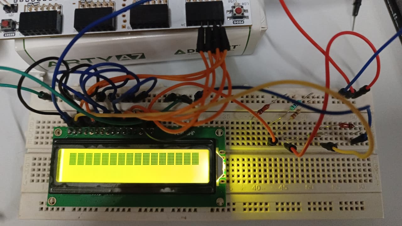
Wiring Table
| LCD Pin | Name | Connect To |
|---|---|---|
| 1 | VSS | GND |
| 2 | VDD | 5V (Arty power header) |
| 3 | V0 | Resistor divider middle |
| 4 | RS | JA Pin 1 |
| 5 | RW | GND (write-only) |
| 6 | E | JA Pin 2 |
| 7–10 | D0–D3 | GND (4-bit mode) |
| 11 | D4 | JA Pin 3 |
| 12 | D5 | JA Pin 4 |
| 13 | D6 | JA Pin 7 |
| 14 | D7 | JA Pin 8 |
| 15 | LED+ | 5V via 100Ω |
| 16 | LED- | GND |
RW is tied permanently to GND. We only write to the LCD, never read. This saves a pin and simplifies the FSM.
*
Verifying Wiring Before Programming
Before touching Vivado, verify with a multimeter:
- LCD pin 1 (VSS): 0V ✓
- LCD pin 2 (VDD): ~4.9V ✓
- LCD pin 3 (V0): ~0.45–0.8V ✓
If the backlight is connected correctly, the LCD should glow green/yellow immediately when the Arty is powered — before any bitstream is loaded. You will also see a row of black filled blocks on the top line. This is the LCD in its default uninitialized state — exactly correct.
Part 4: The FSM Design
The entire LCD controller is one finite state machine running off the 100MHz system clock.
Clock architecture:
The 100MHz clock is divided down to 1MHz ticks (1µs resolution) using a simple counter. All timing in the FSM is measured in microseconds by counting these ticks.
100MHz clock → divide by 100 → 1µs tick pulse
FSM overview:
POWER_ON_WAIT (50ms)
    ↓
INIT sequence (3× 0x3, then 0x2 for 4-bit mode)
    ↓
FUNCTION SET (0x28)
    ↓
DISPLAY ON (0x0C)
    ↓
CLEAR DISPLAY (0x01) ← 2ms wait
    ↓
ENTRY MODE (0x06)
    ↓
WRITE LINE 1 (16 chars, 2 nibbles each)
    ↓
SET DDRAM ADDRESS to line 2 (0xC0)
    ↓
WRITE LINE 2 (16 chars)
    ↓
DONE (hold forever)
4-bit write sequence for every command/character:
Each byte is sent as two nibbles with Enable pulses:
1. Set RS (0=command, 1=data)
2. Put high nibble [7:4] on D4-D7
3. Pulse E high → wait 1µs → E low
4. Wait 1µs
5. Put low nibble [3:0] on D4-D7
6. Pulse E high → wait 1µs → E low
7. Wait execution time (50µs normal, 2000µs for Clear)
Moving to line 2:
The HD44780 uses a DDRAM address space where line 1 starts at 0x00 and line 2 starts at 0x40. To move the cursor, send a Set DDRAM Address command: 0x80 | 0x40 = 0xC0. This is sent as a command (RS=0) like any other.
Part 5: The Code
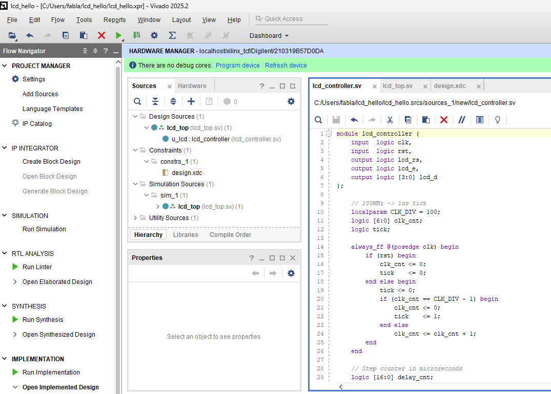
lcd_controller.sv
This is the core FSM. It takes the 100MHz clock and reset as inputs and drives the 6 LCD signal lines.
Key design decisions:
delay_topregister is set by each state to define how long to waitnext_stateregister allows a generic WAIT state to return to any state- Command sequencing uses a
cmd_byteregister so one set of states handles all commands - Character data is stored in a 32-entry ROM (16 chars × 2 lines)
module lcd_controller (
    input  logic clk,        // 100MHz
    input  logic rst,
    output logic lcd_rs,
    output logic lcd_e,
    output logic [3:0] lcd_d
);

    // 100MHz -> 1us tick
    localparam CLK_DIV = 100;
    logic [6:0] clk_cnt;
    logic tick;

    always_ff @(posedge clk) begin
        if (rst) begin
            clk_cnt <= 0; tick <= 0;
        end else begin
            tick <= 0;
            if (clk_cnt == CLK_DIV - 1) begin
                clk_cnt <= 0; tick <= 1;
            end else clk_cnt <= clk_cnt + 1;
        end
    end

    logic [16:0] delay_cnt, delay_top;
    logic        delay_done;

    always_ff @(posedge clk) begin
        if (rst) begin
            delay_cnt <= 0; delay_done <= 0;
        end else begin
            delay_done <= 0;
            if (tick) begin
                if (delay_cnt >= delay_top - 1) begin
                    delay_cnt <= 0; delay_done <= 1;
                end else delay_cnt <= delay_cnt + 1;
            end
        end
    end

    typedef enum logic [6:0] {
        S_IDLE, S_WAIT,
        S_INIT1, S_INIT2, S_INIT3, S_INIT4,
        S_CMD_HI, S_CMD_HI_HOLD, S_CMD_HI_LOW,
        S_CMD_LO_HOLD, S_CMD_WAIT,
        S_CHR_HI, S_CHR_HI_HOLD, S_CHR_HI_LOW,
        S_CHR_LO_HOLD, S_CHR_WAIT,
        S_NEXT_CHAR, S_DONE
    } state_t;

    state_t     state, next_state;
    logic [7:0] cmd_byte;
    logic [4:0] char_idx;
    logic       doing_line2;

    // Message ROM — Line 1: "Hello World!    " / Line 2: "Using FPGA      "
    logic [7:0] msg [0:31];
    initial begin
        msg[0]=8'h48; msg[1]=8'h65; msg[2]=8'h6C; msg[3]=8'h6C;
        msg[4]=8'h6F; msg[5]=8'h20; msg[6]=8'h57; msg[7]=8'h6F;
        msg[8]=8'h72; msg[9]=8'h6C; msg[10]=8'h64; msg[11]=8'h21;
        msg[12]=8'h20; msg[13]=8'h20; msg[14]=8'h20; msg[15]=8'h20;
        msg[16]=8'h55; msg[17]=8'h73; msg[18]=8'h69; msg[19]=8'h6E;
        msg[20]=8'h67; msg[21]=8'h20; msg[22]=8'h46; msg[23]=8'h50;
        msg[24]=8'h47; msg[25]=8'h41; msg[26]=8'h20; msg[27]=8'h20;
        msg[28]=8'h20; msg[29]=8'h20; msg[30]=8'h20; msg[31]=8'h20;
    end

    // Full FSM in repository — handles power-on wait, 3-step init,
    // 4-bit mode switch, function set, display on, clear,
    // entry mode, char writes, line 2 cursor move

endmodule
lcd_top.sv
Thin wrapper connecting the system clock and button reset to the controller:
module lcd_top (
    input  logic clk,
    input  logic [3:0] btn,
    output logic lcd_rs,
    output logic lcd_e,
    output logic [3:0] lcd_d
);
    lcd_controller u_lcd (
        .clk    (clk),
        .rst    (btn[0]),
        .lcd_rs (lcd_rs),
        .lcd_e  (lcd_e),
        .lcd_d  (lcd_d)
    );
endmodule
BTN0 on the Arty acts as reset — press it to restart the init sequence.
design.xdc
## Clock — 100MHz
set_property -dict { PACKAGE_PIN E3 IOSTANDARD LVCMOS33 } [get_ports { clk }]
create_clock -add -name sys_clk_pin -period 10.00 [get_ports { clk }]

## Button 0 — reset
set_property -dict { PACKAGE_PIN D9 IOSTANDARD LVCMOS33 } [get_ports { btn[0] }]

## JA Pmod — LCD signals
set_property -dict { PACKAGE_PIN G13 IOSTANDARD LVCMOS33 } [get_ports { lcd_rs }]
set_property -dict { PACKAGE_PIN B11 IOSTANDARD LVCMOS33 } [get_ports { lcd_e  }]
set_property -dict { PACKAGE_PIN A11 IOSTANDARD LVCMOS33 } [get_ports { lcd_d[0] }]
set_property -dict { PACKAGE_PIN D12 IOSTANDARD LVCMOS33 } [get_ports { lcd_d[1] }]
set_property -dict { PACKAGE_PIN D13 IOSTANDARD LVCMOS33 } [get_ports { lcd_d[2] }]
set_property -dict { PACKAGE_PIN B18 IOSTANDARD LVCMOS33 } [get_ports { lcd_d[3] }]
Critical note on XDC: Vivado will refuse bitstream generation if any top-level port is unconstrained. Every single port in your top module must have a corresponding constraint. This was the cause of the first build failure in this project.
Part 6: Vivado Project Setup
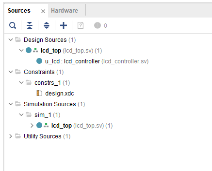
Source file structure:
Design Sources
└── lcd_top (lcd_top.sv)        ← set as top
    └── u_lcd : lcd_controller (lcd_controller.sv)

Constraints
└── design.xdc
Common mistake: Vivado sometimes places a file in Simulation Sources instead of Design Sources when you add it. Always check the Sources panel — your top module must be under Design Sources and shown in bold.
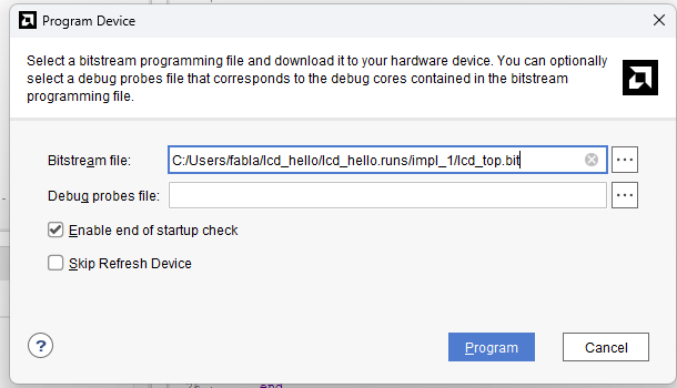
Build flow:
- Flow Navigator → Generate Bitstream (runs synthesis + implementation automatically)
- Open Hardware Manager → Auto Connect
- Program Device
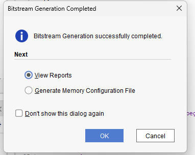
Build time on the A7-100T: approximately 3–5 minutes.
Part 7: Debugging Journey
Getting to a working display was not one shot. Here is what broke and why.
Failure 1 — Bitstream generation failed: unconstrained port rst
Error:
[DRC NSTD-1] Unspecified I/O Standard: Problem ports: rst
[DRC UCIO-1] Unconstrained Logical Port: Problem ports: rst
Cause: The first version of lcd_top.sv declared rst as a separate input port. Vivado saw it as a top-level pin with no XDC entry.
Fix: Remove rst as a port. Connect btn[0] directly to the controller’s .rst input inside the instantiation. rst becomes an internal wire — Vivado stops complaining.
Lesson: Every port in your top module equals one physical pin. If you do not assign it in XDC, the build fails.
Failure 2 — Bitstream generated but LCD showed nothing
The LCD cleared (black boxes disappeared after programming) but no text appeared.
Cause: The original FSM had a logic bug — lcd_e was being set in the same always block cycle where wait_done was being checked. In synchronous logic, you cannot read and respond to a signal in the same clock edge it is generated. The Enable pulse was either missing or incorrectly timed.
Fix: Complete FSM rewrite with explicit separate states for setting up data lines, asserting Enable high, holding Enable, deasserting Enable, and waiting execution time. Each transition is one clock edge minimum.
Lesson: In synchronous HDL, every action takes at least one clock cycle. Separate “set” and “check” into different states.
Failure 3 — Vivado using wrong top module
After moving lcd_top.sv to Design Sources, Vivado still showed lcd_controller as the top module.
Cause: Vivado caches the top module setting. Moving a file does not automatically promote it to top.
Fix: Right-click lcd_top in Sources → Set as Top. Confirm it appears bold.
Part 8: It Works
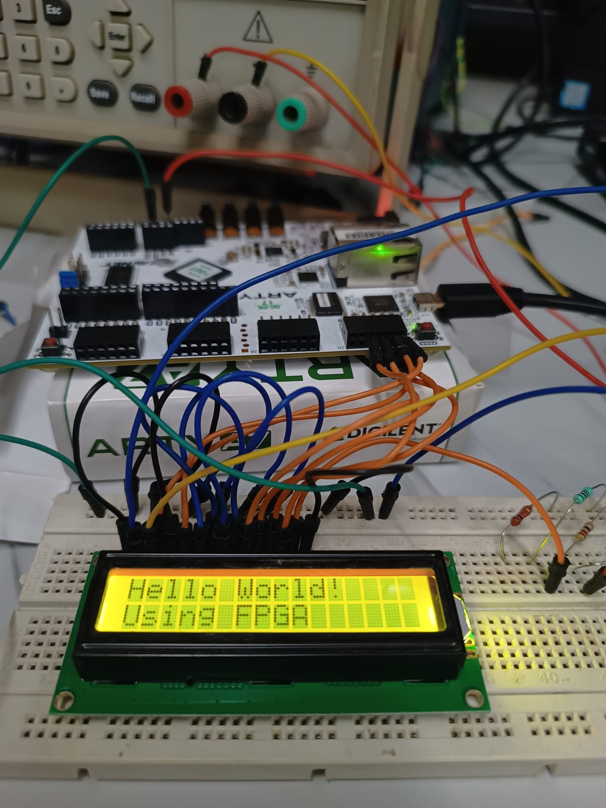
After flashing the corrected bitstream, the LCD initialized cleanly and displayed both lines of text. Pressing BTN0 restarts the sequence — the display clears and rewrites from scratch.
What is actually happening at the hardware level:
- Power on → FPGA starts FSM at
S_IDLE - 50ms wait → HD44780 internal power-on reset completes
- 3-step 8-bit preamble → HD44780 enters known state
- Switch to 4-bit mode → all communication now uses 2 nibbles per byte
- Function set, display on, clear, entry mode → LCD ready
- 16 characters × 2 nibbles each → “Hello World!” appears on line 1
- DDRAM address set to 0x40 → cursor jumps to line 2
- 16 more characters → “Using FPGA” appears on line 2
- FSM reaches
S_DONE→ holds, LCD freezes on the message
Total time from reset to text displayed: approximately 55ms — imperceptible to a human.
Part 9: Key Lessons
1. Timing is everything with HD44780
The datasheet timing values are minimums, not suggestions. The LCD’s internal processor runs at roughly 270kHz. It needs hundreds of microseconds to execute a command. Send the next command too early and the LCD ignores it silently — no error, just missing characters.
2. The initialization sequence cannot be skipped
The 3-step 8-bit preamble before switching to 4-bit mode is mandatory. It exists because the LCD has no reset pin and the internal state machine could be anywhere after power-on. The preamble forces it into a known state regardless of where it started.
3. Separate your clock domain from your timing logic
Running the FSM directly off 100MHz and counting cycles is possible but error-prone. Generating a 1µs tick pulse and counting ticks keeps the code readable and the timing obvious.
4. XDC constraints are not optional
Vivado enforces complete pin assignment. Every port in your top module must have a corresponding XDC entry. Budget time to get this right before trying to build.
5. FSM state separation
Each physical action needs its own state. Trying to compress multiple actions into one state creates race conditions. Assert Enable in one state. Check done in the next. Never both in the same state.
Part 10: What Is Next
This LCD controller is now a reusable module. Immediate next steps:
- Display ALU results: Connect the 8-bit ALU so switch inputs drive operands, op-code selects operation, and the result displays as decimal on the LCD
- UART to LCD bridge: Receive characters over UART from a PC and display them in real time — turns the display into a serial terminal
- Scrolling message: Implement the HD44780 scroll command to animate long strings across the display
Technical Specifications
| Parameter | Value |
|---|---|
| FPGA | Xilinx Artix-7 (XC7A100T) |
| Board | Digilent Arty A7-100T |
| Tool | Vivado 2025.2 |
| HDL | SystemVerilog |
| LCD | HD44780 16×2 green backlight |
| Interface | 4-bit parallel |
| Clock | 100MHz system clock |
| LCD VDD | 5V |
| FPGA I/O | 3.3V LVCMOS |
| Contrast V0 | ~0.45V (10K + 1K divider) |
| Pmod used | JA |
| Init time | ~55ms after reset |
| Build time | ~4 minutes |
This post is part of an ongoing FPGA learning series on IoTSec.
Happy Learning!